




The Semiconductor Manufacturing Challenge: Yield at the Atomic Scale
Modern semiconductor fabrication is arguably the most complex manufacturing process in human history. As logic nodes shrink to 3nm and below, and 3D NAND memory stacks exceed 200+ layers, the physical tolerances inside fabrication tools are measured in angstroms. In this environment, micro-particle contamination and plasma-induced tool wear are the primary enemies of wafer yield.
Inside plasma etch chambers, reactive gases (like CF₄, CHF₃, Cl₂, and HBr) are energized into aggressive plasmas that physically and chemically strip away material. Conventional metals would instantly corrode, and standard polymers would melt or outgas. While silicon and quartz (SiO₂) are commonly used, they suffer from rapid erosion rates or brittleness. High-purity Silicon Nitride (Si₃N₄) has emerged as the critical advanced ceramic material that bridges the gap, offering the ultimate combination of plasma resistance, mechanical toughness, and ultra-low particle generation required for advanced node fabs.
Key Si₃N₄ Properties for Cleanroom Environments
| Property | Si₃N₄ Value | Semiconductor Significance |
|---|---|---|
| Purity Level | > 99.99% (4N) | Prevents metallic/mobile ion wafer contamination |
| Plasma Erosion Resistance | Exceptional | Survives aggressive CF₄/O₂ and halogen plasmas |
| Particle Generation | Ultra-Low | Minimizes wafer defect density (improves yield) |
| Fracture Toughness (KIC) | 6-8 MPa·m½ | Prevents catastrophic shattering during robotic wafer handling |
| Flexural Strength | 700-1000 MPa | Supports heavy wafer loads in furnace boats without sagging |
| Thermal Shock (ΔT) | > 800°C | Survives rapid heating/cooling in CVD/Diffusion furnaces |
The Role of Si₃N₄ Focus Rings in Plasma Etch Chambers
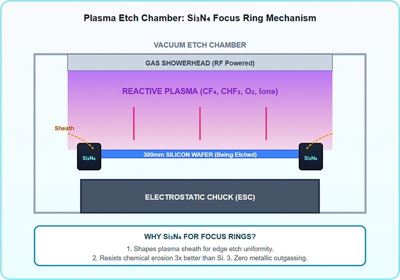
The most critical application of Si₃N₄ in the fab is the Focus Ring (or Edge Ring) in dielectric and conductor etch tools. This ring surrounds the silicon wafer, shaping the plasma sheath to ensure uniform etching at the wafer's extreme edge. The diagram below illustrates how Si₃N₄ outperforms silicon in this brutal environment:
Diagram 1: Plasma Etch Chamber & Si₃N₄ Focus Ring Cross-div
The Edge Effect Problem
At the extreme edge of a 300mm wafer, the plasma sheath naturally bends, causing uneven ion bombardment and poor etch uniformity. The Si₃N₄ focus ring acts as a physical and electrical boundary that forces the plasma sheath to remain perfectly horizontal across the entire wafer surface, ensuring critical dimension (CD) uniformity from center to edge.
Particle Defect Prevention
If a focus ring erodes too quickly (like Silicon or Quartz), it flakes off micro-particles that land on the wafer, killing the microchips. High-density, high-purity Si₃N₄ erodes uniformly and slowly, reducing particle adder defects by up to 80% compared to standard materials, directly boosting fab yield.
Core Applications of Si₃N₄ in the Fab
1. Plasma Etch Focus Rings & Showerheads
Role: Defines the plasma boundary around the wafer; distributes reactive gases.
Si₃N₄ Advantage: Superior resistance to fluorocarbon and halogen plasmas. Maintains precise dimensional tolerances over thousands of RF hours, ensuring consistent etch profiles for 3D NAND high-aspect-ratio holes.
2. CMP Retaining Rings & Dressers
Role: Holds the wafer carrier pad in place during Chemical Mechanical Planarization (CMP); conditions the polishing pad.
Si₃N₄ Advantage: Extreme hardness (HV 15 GPa) and high fracture toughness prevent chipping under high down-force pressure. Does not contaminate the highly sensitive CMP slurry with metallic ions.
3. Diffusion & LPCVD Wafer Boats
Role: Holds 100+ wafers vertically inside high-temperature (up to 1200°C) oxidation and CVD furnaces.
Si₃N₄ Advantage: Zero high-temperature creep (sagging). Unlike Quartz boats that warp over time and cause wafer slipping, Si₃N₄ boats remain perfectly rigid, preventing catastrophic wafer breakage during robotic loading.
4. Lithography & Inspection Stages
Role: Structural components, mirrors, and motion stages in EUV/DUV lithography and wafer inspection tools.
Si₃N₄ Advantage: Exceptional specific stiffness (stiffness-to-weight ratio) and low thermal expansion. Enables ultra-high-speed stage acceleration without vibration, ensuring nanometer-level overlay accuracy.
Si₃N₄ Deployment Across the Fab Process Flow
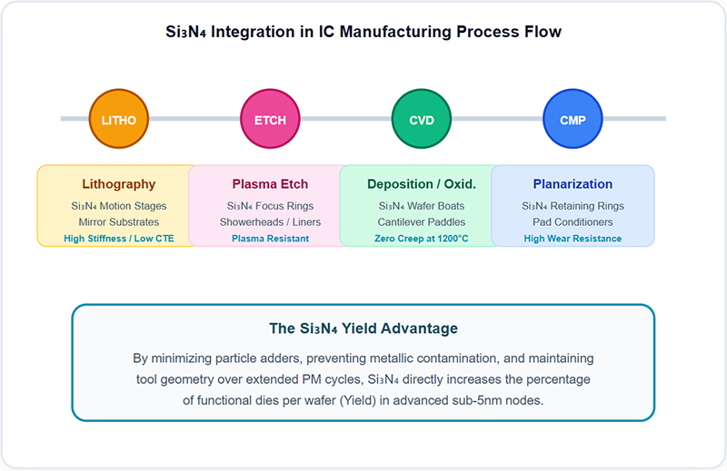
The following diagram maps the integration of Si₃N₄ ceramic components across the major steps of the semiconductor front-end-of-line (FEOL) and back-end-of-line (BEOL) manufacturing flow:
Diagram 2: Si₃N₄ Components in the Semiconductor Process Flow
Yield and Cost Advantages for Fabs
Increased Wafer Yield
In advanced nodes, a single micro-particle can kill a multi-million-dollar wafer lot. Si₃N₄'s ultra-low particle generation and lack of metallic impurities directly translate to higher yield percentages, generating millions in additional revenue per tool per year.
Extended PM Cycles
Every time a tool is opened for Preventive Maintenance (PM) to replace worn focus rings, the fab loses 12-24 hours of production. Si₃N₄'s slow erosion rate allows PM intervals to be extended by 30-50%, drastically improving Overall Equipment Effectiveness (OEE).
Tool Protection
Unlike brittle Quartz (SiO₂) which can shatter during robotic wafer transfers and damage the ESC, Si₃N₄'s high fracture toughness (6-8 MPa·m½) ensures it survives accidental impacts, protecting multi-million-dollar chamber internals.
Etch Chamber Material Comparison: Si₃N₄ vs Alternatives
| Property | Si₃N₄ (High Purity) | Silicon (Si) | Quartz (SiO₂) | Al₂O₃ | SiC (CVD) |
|---|---|---|---|---|---|
| Plasma Erosion Rate | Very Low ★ | High | Moderate | Low | Very Low |
| Fracture Toughness | High (6-8) ★ | Low (~1) | Very Low (~0.8) | Low (3-4) | Low (3-4) |
| Particle Generation | Ultra-Low ★ | Moderate | High (Flaking) | Moderate | Low |
| Electrical Conductivity | Insulator | Semiconductor | Insulator | Insulator | Semiconductor |
| Relative Cost | High | Medium | Low | Medium | Very High |
★ Best balance of properties for Focus Rings. While CVD SiC offers excellent plasma resistance, its high cost and lower toughness make Si₃N₄ the preferred choice for many high-volume etch applications where impact resistance and cost-efficiency are critical.
Why Partner With HUACIJULI for Semiconductor Si₃N₄?
Ultra-High Purity Sintering
Proprietary GPS/HIP sintering processes using 4N+ raw powders. Strict control of metallic impurities to the ppb level, ensuring zero mobile ion contamination in your fab.
Cleanroom-Ready Finishing
Precision CNC grinding and lapping in ISO Class 6/7 cleanroom environments. Parts are ultrasonically cleaned and vacuum-packed to prevent particulate contamination during transit.
Complex Geometry Mastery
5-axis machining capabilities to produce complex focus ring profiles, gas showerhead hole patterns, and delicate wafer boat cantilevers to micrometer tolerances.
Optimizing Your Fab Yield and PM Cycles?
Send us your tool drawings and plasma chemistry specs. Our semiconductor materials team will engineer a custom high-purity Si₃N₄ solution to outperform your current consumables.
Request Semiconductor Engineering ConsultationFrequently Asked Questions (FAQ)
Q1: Why use Si₃N₄ instead of Silicon for plasma etch focus rings?
While Silicon is conductive and cheap, it etches rapidly in fluorine-based plasmas, requiring frequent replacement and generating high particle counts. Si₃N₄ is significantly more chemically resistant to these plasmas, lasting 2-3 times longer, reducing PM downtime, and drastically lowering the particle defect rate on the wafer edge.
Q2: How does Si₃N₄ prevent wafer contamination?
Semiconductor-grade Si₃N₄ is manufactured to >99.99% purity. Alkali metals (like Na and K) and heavy metals are strictly controlled at the ppb level. This prevents mobile ion contamination, which can shift transistor threshold voltages and cause catastrophic device failure. Furthermore, its high toughness prevents the micro-chipping and flaking that plagues brittle Quartz parts.
Q3: Why are Si₃N₄ wafer boats preferred over Quartz in CVD furnaces?
In high-temperature CVD and oxidation furnaces (up to 1200°C), Quartz (SiO₂) boats slowly sag and warp due to high-temperature creep. This warping causes wafers to slip, stick, or break during robotic unloading. Si₃N₄ exhibits virtually zero creep at 1200°C, maintaining perfect dimensional stability and preventing costly wafer breakage incidents over thousands of thermal cycles.
Q4: Can Si₃N₄ be used in CMP (Chemical Mechanical Planarization)?
Yes. Si₃N₄ is widely used for CMP retaining rings. The retaining ring holds the wafer carrier pad in place under high down-force. Si₃N₄'s extreme hardness (HV 15 GPa) and high fracture toughness prevent the ring from wearing down or chipping, ensuring uniform polishing pressure across the wafer and preventing slurry contamination.