
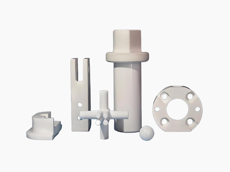
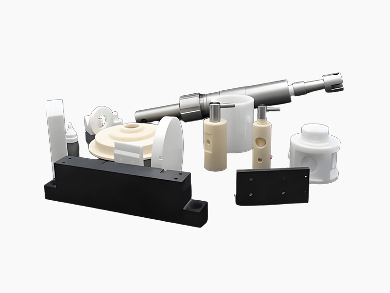


Semiconductor manufacturing requires extreme precision at the micron and even nanometer level. In such environments, even the smallest alignment deviation can result in defective wafers. This is where the silicon nitride ceramic centering pin becomes indispensable.
Challenges in Semiconductor Alignment
Semiconductor tools operate under:
High temperatures
Vacuum environments
Chemical exposure
Traditional metal pins often fail due to thermal expansion and corrosion, leading to alignment instability.
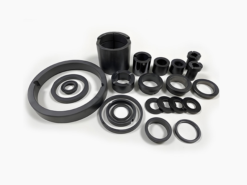
Why Silicon Nitride Is Ideal
Silicon nitride ceramic centering pins offer:
Non-magnetic properties
Chemical inertness
High stiffness
These characteristics ensure stable performance in sensitive semiconductor processes such as lithography and wafer handling.
Impact on Yield and Productivity
Accurate centering directly affects:
Wafer positioning accuracy
Equipment repeatability
Yield rates
By minimizing alignment errors, silicon nitride pins help manufacturers achieve higher throughput and lower defect rates.
Cleanroom Compatibility
Another advantage is the material’s low particle generation. In cleanroom environments, contamination control is critical. Silicon nitride surfaces generate fewer particles compared to metals, making them ideal for ultra-clean applications.
Conclusion
For semiconductor manufacturers aiming to enhance precision and reliability, silicon nitride ceramic centering pins provide a robust and future-proof solution.