




Beyond Incremental Improvement: A Paradigm Shift
For decades, silicon nitride advancement followed a predictable trajectory: optimize sintering aids, refine grain morphology, improve density. These incremental gains delivered reliable, high-performance materials-but they are approaching asymptotic limits. The next decade belongs to paradigm-shifting innovations that fundamentally redefine what Si₃N₄ can do.
This article synthesizes cutting-edge research, industrial R&D roadmaps, and emerging commercial deployments to map the five converging trends that will define advanced Si₃N₄ structural ceramics through 2035. Each trend represents not just a technical improvement, but an expansion of the material's application envelope into domains previously considered impossible.
Trend 1: Nano-Engineered Grain Boundary Design
The grain boundary phase has historically been Si₃N₄'s Achilles' heel-the weakest link for corrosion, creep, and thermal conductivity. Next-generation materials science is transforming this liability into a designable nano-architectural feature through precise rare-earth oxide chemistry and controlled devitrification kinetics.
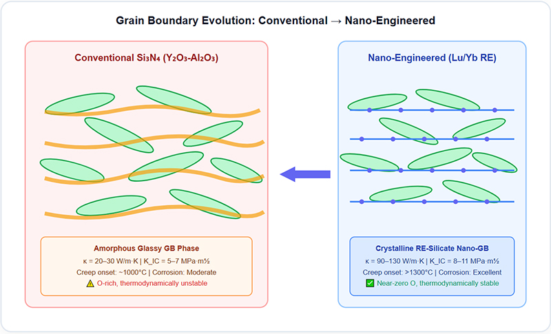
Diagram 1: Evolution of Si₃N₄ Grain Boundary Architecture
Heavy Rare-Earth Oxide Chemistry
Lutetium (Lu₂O₃) and Ytterbium (Yb₂O₃) have smaller ionic radii than Yttrium, producing crystalline grain boundary silicates (Lu₂Si₂O₇, Yb₂Si₂O₇) with higher melting points (>1900°C), lower oxygen diffusivity, and superior phonon transmission. This simultaneously raises creep resistance by 200°C and thermal conductivity by 3–4× versus conventional Y-Al-Si-O-N glass.
Dual-Property Optimization
Historically, toughness and thermal conductivity were inversely correlated in Si₃N₄. Nano-engineered GB breaks this trade-off: crystalline RE-silicate boundaries provide both crack-deflection toughening (via elastic mismatch at coherent interfaces) and efficient phonon transport (via ordered crystal structure). This enables single-material solutions for applications previously requiring composite designs.
Trend 2: Additive Manufacturing of Complex Si₃N₄ Geometries
Silicon nitride's extreme hardness makes subtractive machining prohibitively expensive for complex geometries. Additive manufacturing (AM) is dismantling this barrier, enabling net-shape production of previously unfabricable architectures while reducing lead times from months to weeks.
Two AM approaches are reaching commercial maturity for Si₃N₄: Lithography-Based Ceramic Manufacturing (LCM/SLA) offers sub-50μm resolution for precision components like micro-turbine rotors and lattice heat exchangers; Binder Jetting enables larger-scale production of porous filters, catalyst supports, and topology-optimized structural brackets. Both require specialized debinding and GPSN post-processing protocols to achieve >99% theoretical density.
Extended Knowledge: The Cost Inflection Point
AM becomes economically advantageous over press-and-machine when component complexity exceeds a threshold defined by the "machining-to-material cost ratio." For simple bearings and seal rings, conventional processing remains cheaper. But for components with internal channels, conformal cooling, or organic topology optimization, AM reduces total cost by 40-60% by eliminating diamond grinding, EDM, and multi-axis CNC operations. Industry analysts project AM-produced Si₃N₄ components will reach 15-20% of total market volume by 2032.
Trend 3: Ultra-High Thermal Conductivity Substrates for Power Electronics
The global transition to electric vehicles, renewable energy, and grid modernization is creating unprecedented demand for power electronic substrates that can handle higher temperatures, higher power densities, and faster switching frequencies. Si₃N₄ is emerging as the definitive substrate material for next-generation SiC and GaN power modules.
Active Metal Brazing (AMB) compatible Si₃N₄ substrates with thermal conductivity of 90-130 W/m·K combine the thermal performance of AlN with 3× higher fracture toughness and superior thermal cycling reliability. Unlike Direct Bonded Copper (DBC) on alumina, AMB-Si₃N₄ survives >30,000 thermal cycles (-40°C to +200°C) without copper delamination or ceramic cracking-enabling the compact, high-reliability inverters that define modern EV drivetrains.
EV Traction Inverters
SiC MOSFET modules at >200°C junction temp require substrates matching SiC CTE (3.2 ppm/K) while extracting 50+ kW/L heat flux. Si₃N₄ AMB enables 30% smaller inverter volume vs. AlN-DBC, directly extending vehicle range.
Solar & Wind Inverters
Utility-scale inverters demand 25-year field reliability under outdoor thermal cycling. Si₃N₄ AMB substrates eliminate the solder fatigue failures plaguing DBC alumina in 1500V string inverters, reducing LCOE by 2-4%.
Fast Charging Stations
350-800 kW DC fast chargers generate extreme transient thermal loads. Si₃N₄'s combination of high κ and high toughness prevents substrate fracture during rapid load transients that crack brittle AlN substrates.
Trend 4: Expanding Frontiers in Aerospace & Electric Mobility
Beyond power electronics, Si₃N₄ is penetrating high-value aerospace and automotive applications where its unique property combination solves previously intractable engineering challenges.
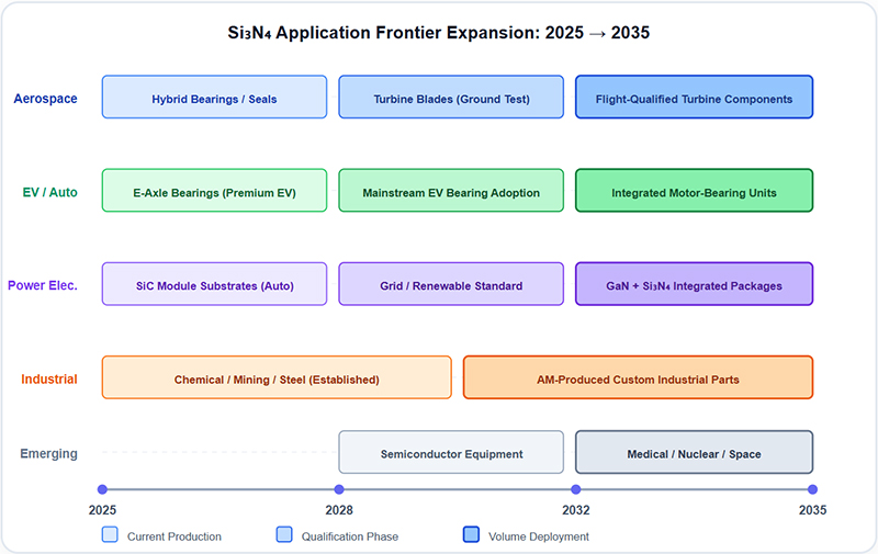
Diagram 2: Si₃N₄ Application Expansion Map (2025-2035)
Aerospace: Oil-Free Turbomachinery
Si₃N₄ turbine components operating at 1350-1400°C eliminate the need for film-cooling air and oil lubrication systems. This improves Brayton cycle efficiency by 5-8%, reduces engine weight by 15-20 kg, and cuts NOx emissions through leaner combustion. AM-enabled internal cooling channels further push operating temperatures toward 1450°C by 2032.
EV: Integrated E-Axle Systems
Next-gen e-axles integrate motor, gearbox, and inverter into a single housing. Si₃N₄ bearings survive the combined electrical, thermal, and mechanical stresses of this integration while being immune to electrical erosion from inverter-induced bearing currents-a failure mode destroying steel bearings in 400V/800V EV platforms within 30,000 km.
Trend 5: Sustainability & Circular Economy Integration
As ESG mandates tighten globally, Si₃N₄ manufacturers are developing sustainable production pathways that reduce carbon footprint without compromising performance. Three initiatives are gaining momentum:
Powder Recycling & Reuse
Green machining swarf and rejected green bodies are being reclaimed via acid leaching and re-milling processes. Recycled powder now achieves >95% virgin-equivalent performance in non-critical applications, reducing raw material waste by 20-30% and embodied carbon by 15-25%.
Electrified Sintering
Transition from gas-fired to electric GPSN furnaces powered by renewable energy reduces Scope 1 emissions by 80-90%. Microwave-assisted sintering reduces cycle times by 40% and energy consumption by 35%, while producing finer grain microstructures with superior mechanical properties.
Bio-Derived Sintering Aids
Research into plant-derived rare-earth precursors and bio-based binder systems for AM feedstocks is advancing rapidly. While not yet commercially deployed, lab-scale results show equivalent densification behavior with 50% lower lifecycle GWP for the additive package.
Technical Frequently Asked Questions
Q1: What are the most significant technological breakthroughs shaping the future of Si₃N₄ ceramics?
Three breakthroughs are redefining Si₃N₄ capabilities: (1) Nano-engineered grain boundary design using rare-earth oxides (Lu₂O₃, Yb₂O₃) that crystallize into refractory intergranular phases with near-zero oxygen content, simultaneously maximizing fracture toughness (>10 MPa·m½) and thermal conductivity (>90 W/m·K); (2) Binder Jetting and SLA-based additive manufacturing enabling net-shape production of complex geometries previously impossible via conventional pressing; (3) AMB-compatible high-purity Si₃N₄ substrates with thermal conductivity exceeding 120 W/m·K, replacing AlN and DBC alumina in next-gen SiC/GaN power modules.
Q2: How will additive manufacturing change silicon nitride component production?
AM eliminates geometric constraints of pressing and CNC machining. Key impacts: (1) Internal cooling channels in turbine blades improving efficiency by 15-25%; (2) Topology-optimized lightweight structures reducing rotating mass by 30-50%; (3) Prototyping cycles reduced from 8-12 weeks to 2-3 weeks; (4) Finishing costs reduced by 40-60% through near-net-shape production. Current challenges include achieving full density post-sintering and managing anisotropic shrinkage, but GPSN-compatible AM feedstocks are reaching commercial maturity.
Q3: Why is high-thermal-conductivity Si₃N₄ critical for electric vehicle power electronics?
Next-gen EV inverters use SiC MOSFETs at junction temperatures >200°C with power densities >50 kW/L. Traditional DBC alumina fails due to low κ (~24 W/m·K) and CTE mismatch-induced solder fatigue. High-κ Si₃N₄ AMB substrates (90-130 W/m·K) match AlN thermally while offering 3× higher fracture toughness, surviving >30,000 thermal cycles without cracking. Their CTE (~3.2 ppm/K) closely matches SiC chips, enabling smaller, lighter, more reliable inverters that directly extend EV range.
Q4: What role does Si₃N₄ play in future aerospace and gas turbine development?
Si₃N₄ enables next-gen gas turbines through three pathways: (1) Turbine blades/vanes at 1350-1400°C (vs. 1100°C for superalloys), improving Brayton efficiency by 5-8% and reducing NOx; (2) Hybrid ceramic bearings in APUs and main shafts eliminating oil systems, reducing weight by 15-20 kg/engine; (3) Hypersonic radomes combining low εᵣ (≈7.9) with Mach 5+ rain erosion resistance. AM accelerates qualification by enabling integrated cooling channel designs previously unfabricable.