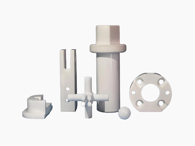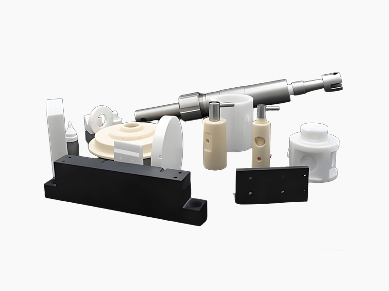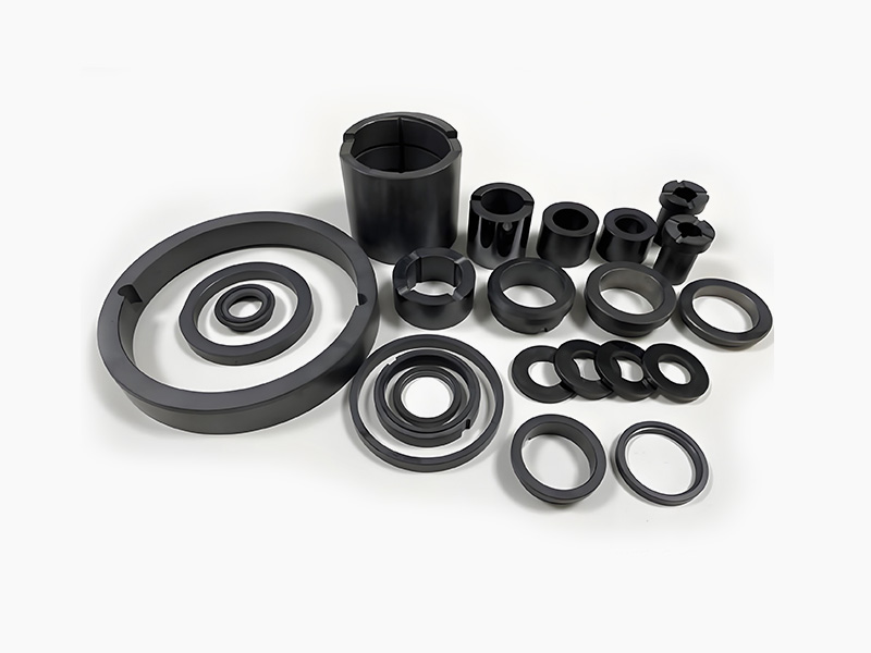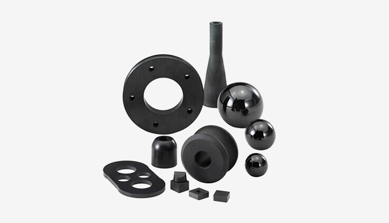
Alumina ceramic wafer handling components are high-precision ceramic parts used in semiconductor manufacturing for wafer transfer, positioning, or support. Their core advantages lie in their high purity, high temperature resistance, corrosion resistance, and excellent insulation properties. The following is a comprehensive analysis of their key characteristics and application scenarios:
Material Characteristics
1. Ultra-high purity: Semiconductor-grade alumina ceramics typically require a purity of ≥99.5% to prevent metal ion contamination (such as iron content <5ppm), ensuring the cleanliness of the wafer processing environment.
2. Resistance to extreme environments: They can withstand temperatures above 1400℃, and their thermal expansion coefficient (6.4-8.2×10⁻⁶/℃) matches that of silicon materials, preventing wafer deformation caused by thermal stress.
3. Corrosion resistance: They exhibit strong corrosion resistance to fluorine-based and chlorine-based gases used in plasma etching, with a service life more than 10 times longer than that of metal components.
Product Design
1. Precision Structure: As part of a wafer handling robot or carrier, it must meet nanometer-level flatness (e.g., ±0.1μm) and low surface roughness (Ra<0.1nm) to prevent wafer scratching.
2. Balance of Insulation and Thermal Conductivity: Dielectric strength ≥15kV/mm, while thermal conductivity is 20-30W/m·K, suitable for the heat dissipation requirements of power devices.
Application Scenarios
1. Etching Equipment: Used as protective components in plasma etching chambers to reduce particle contamination and extend maintenance cycles.
2. Wafer Handling: Used as vacuum suction cups or robotic arm grippers to stably transfer wafers in a vacuum environment, preventing contamination.
3. Packaging and Testing: Used as load-bearing and fixing components in high-temperature packaging processes to ensure wafer positioning accuracy.
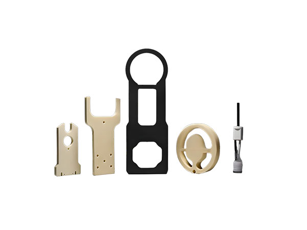
Supports custom specifications.