Semiconductor alumina ceramic chambers, as core components of high-density plasma etching equipment, require designs and applications that meet multiple performance requirements under extreme process environments.
Material Characteristics and Preparation Requirements
1. High Purity and Low Impurities: The alumina ceramic must have a purity of ≥99.9%, with metal impurity content (such as MgO, CaO, and SiO₂) controlled within 0.05%-0.8% to reduce the risk of particle contamination during the plasma etching process.
2. Densification Process: Isostatic pressing and high-temperature sintering (density ≥3.98 g/cm³) are used, and a nanoscale coating (5-10 μm thick) is applied to enhance surface densification, allowing the etching rate to be controlled below 0.1 μm/h.
3. Thermal Stability Matching: The coefficient of thermal expansion (4.2 × 10⁻⁶/℃) must be compatible with the metal substrate (such as aluminum alloy) to prevent coating cracking at high temperatures (300℃) and subsequent chamber failure.
Key Performance Advantages
1. Plasma Erosion Resistance: In CF₄ and SF₆ plasma environments, the corrosion rate of high-purity alumina is reduced by more than 90% compared to traditional metal materials, effectively reducing metal ion contamination of wafers.
2. Dielectric Stability: The dielectric constant is stable under radio frequency electric fields (ε≈9.8), ensuring a plasma distribution uniformity deviation of <±3%, and improving the etching profile verticality to ≥89.5°.
3. Surface Cleanliness Control: After polishing, the surface roughness Ra is <0.2μm, and the porosity is <0.1%, suppressing gas adsorption and particle shedding, meeting the cleanliness requirements for processes below 7nm.
Application Scenarios
1. Etching Chamber Protection: Used as a chamber liner or independent chamber material in equipment from companies such as Lam Research and AMEC, it can withstand highly corrosive gases such as Cl₂ and NF₃, extending its lifespan to over 2000 hours.
2. Gas Delivery System: Used in gas distribution pipes and showerheads, its precise pore structure (pore size 50-100μm) achieves a gas flow rate error of <1%, ensuring etching uniformity.
3. Wafer Support Components: Combined with silicon carbide composite materials for electrostatic chuck substrates, it achieves wafer temperature uniformity of ±0.3℃ at 150℃, with edge warping <10μm.
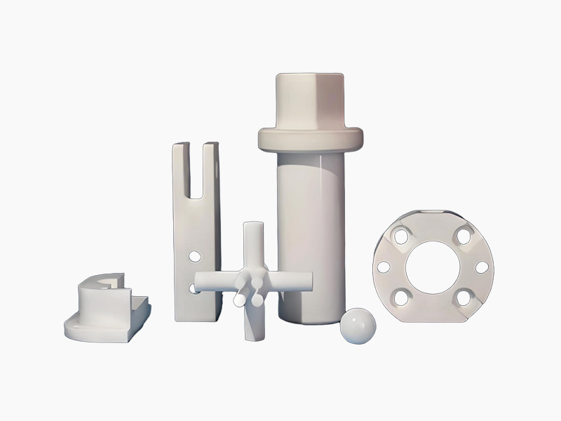
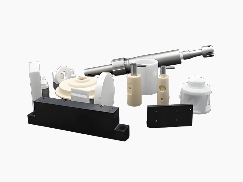
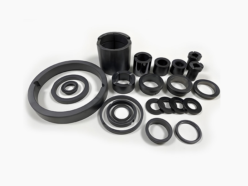
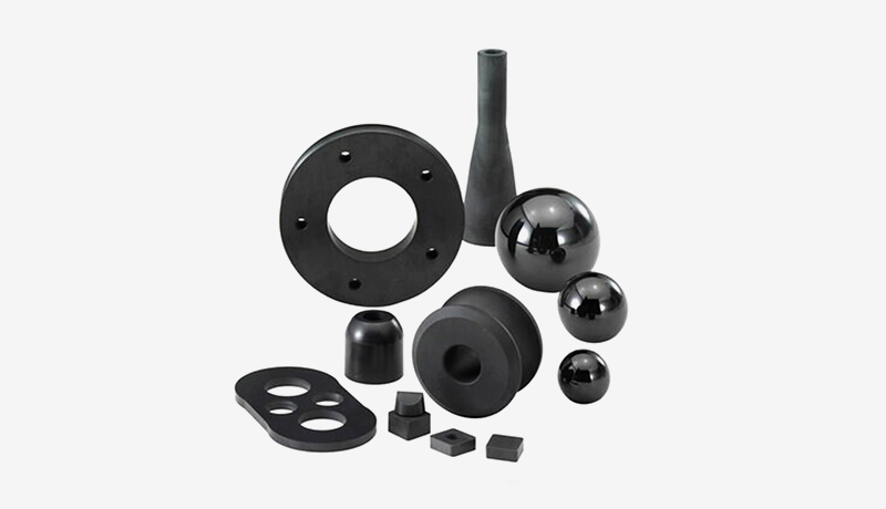
Supports custom specifications.