




Introduction: The Critical Role of Ceramics in Semiconductor Manufacturing
The global semiconductor industry is the backbone of modern technology - powering everything from smartphones and cloud computing to artificial intelligence, autonomous vehicles, and quantum information systems. As semiconductor devices shrink toward sub-3nm process nodes and advanced 3D packaging architectures, the manufacturing equipment and materials used in fabrication must meet increasingly extreme performance requirements.
In this high-stakes environment, silicon nitride (Si₃N₄) ceramics have emerged as one of the most strategically important advanced materials in semiconductor equipment design. Unlike conventional metals, polymers, or even other ceramics, Si₃N₄ delivers a uniquely balanced combination of plasma erosion resistance, chemical inertness, thermal stability, mechanical toughness, and ultra-low particle generation - all of which are non-negotiable requirements in modern wafer fabrication facilities (fabs).
This comprehensive technical guide explores in detail how silicon nitride ceramics are applied across the semiconductor equipment value chain - from plasma etching chambers and CVD/PVD deposition systems to lithography alignment mechanisms, CMP processing, and cleanroom automation. By understanding the material science behind Si₃N₄ and its specific advantages in semiconductor environments, engineers and procurement professionals can make better-informed material selection decisions for next-generation fab equipment.
Silicon Nitride (Si₃N₄) - Material Fundamentals
Silicon nitride is a non-oxide advanced ceramic composed of silicon and nitrogen atoms bound together in a dense, three-dimensional covalent network. First synthesized in 1857 by Henri Étienne Sainte-Claire Deville and Friedrich Wöhler, Si₃N₄ has evolved over the past seven decades into one of the most technologically significant engineering ceramics, particularly in semiconductor, aerospace, and automotive applications.
Flexural Strength
700-1000 MPa
Max Temperature
Up to 1400°C
Fracture Toughness
6-8 MPa·m½
Density
3.17-3.44 g/cm³
Crystal Phases
Si₃N₄ exists in three phases: α-phase (hexagonal, low-temperature synthesis product), β-phase (hexagonal, thermodynamically stable, preferred for engineering ceramics), and γ-phase (cubic spinel-type, only at extreme pressures >15 GPa). The β-phase features elongated, interlocking grains that create natural toughening through crack-bridging mechanisms.
Semiconductor-Grade Purity
For semiconductor applications, Si₃N₄ must achieve ultra-high purity (>99.9%) with controlled trace metallic impurities (<1 ppm for Fe, Cu, Na, K). The material must generate minimal particulate contamination during plasma exposure and wet chemical cleaning cycles, meeting SEMI (Semiconductor Equipment and Materials International) standards for fab use.
Molecular & Crystal Structure of Si₃N₄
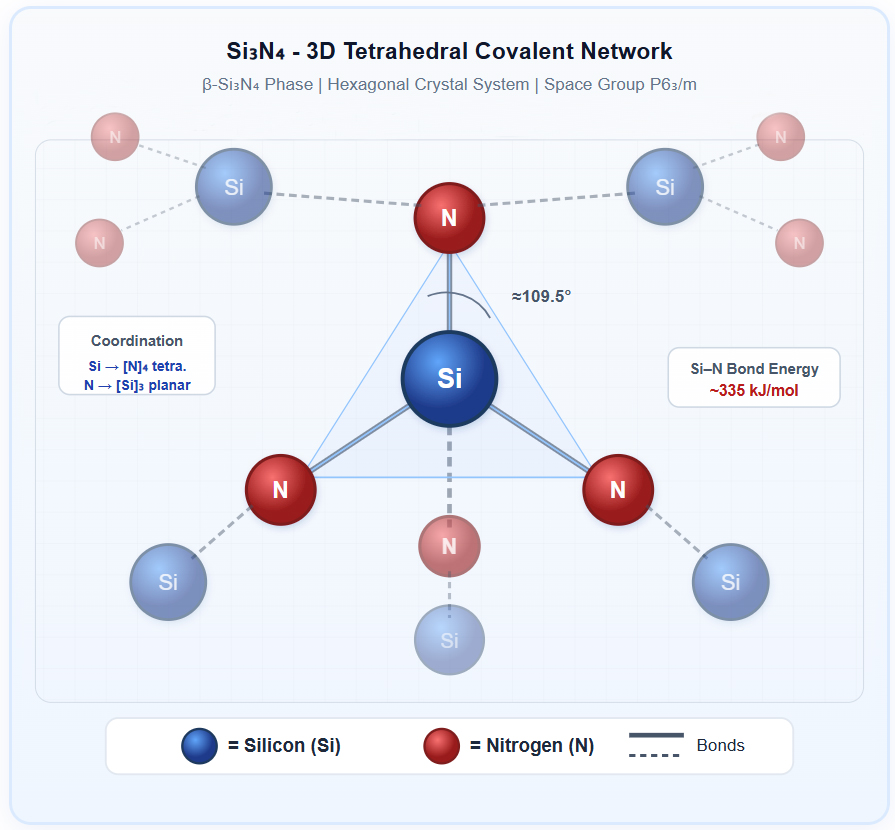
The exceptional performance of silicon nitride in semiconductor environments originates from its unique atomic-level architecture. The Si₃N₄ crystal is constructed from a three-dimensional network of SiN₄ tetrahedra, where each silicon atom is covalently bonded to four nitrogen atoms (sp³ hybridization), and each nitrogen atom bridges three silicon atoms in a planar trigonal configuration. This dense covalent network is the fundamental source of the material's high hardness, chemical inertness, and resistance to plasma erosion - properties that are essential in semiconductor fabrication equipment.
Structure-Property Link for Semiconductors
The strong Si-N covalent bonds (335 kJ/mol) and absence of weak interlayer planes give Si₃N₄ exceptional resistance to plasma erosion - a critical factor in etch chambers where components are bombarded by high-energy ions and reactive radicals. The material erodes 3-10× slower than quartz and comparable to high-purity alumina in fluorine-based plasmas.
Relevance to Semiconductor Processes
The dense 3D network also ensures minimal outgassing under vacuum and ultra-low particle generation during plasma exposure - both critical for maintaining wafer yield in sub-5nm fabrication nodes. Additionally, the chemical similarity to silicon (the substrate material itself) makes Si₃N₄ inherently compatible with Si-based process chemistries.
Why Silicon Nitride for Semiconductor Equipment?
Semiconductor fabrication represents one of the most technically demanding manufacturing environments on Earth. Process chambers operate under extreme conditions - high-energy plasmas, corrosive gases, ultra-high vacuum, rapid thermal cycling, and nanometer-scale precision requirements. Si₃N₄ ceramics meet these challenges through six key advantages:
Plasma Erosion Resistance
In dry etching processes (RIE, DRIE, ICP), chamber components are continuously bombarded by high-energy ions and reactive plasma species (CF₄, SF₆, Cl₂, HBr). Si₃N₄ demonstrates exceptional resistance to plasma erosion, with erosion rates 3-10× lower than quartz and comparable to high-purity Al₂O₃ and AlN in fluorine-based plasmas. This extends component lifetime and reduces particle contamination on wafers.
Ultra-Low Particle Generation
Particle contamination is the #1 yield killer in semiconductor fabs. At sub-7nm nodes, even a single 20nm particle can destroy a transistor. Si₃N₄ generates significantly fewer particles than metal or polymer components during plasma exposure and thermal cycling, helping fabs maintain yield rates above 90% in advanced process steps.
Thermal Stability & Shock Resistance
CVD and diffusion processes operate at 400–1200°C with frequent thermal cycling. Si₃N₄'s low CTE (3.2 × 10⁻⁶/°C) and high thermal shock resistance allow it to endure thousands of rapid heating/cooling cycles without cracking, warping, or dimensional drift - critical for maintaining process repeatability and equipment uptime.
Chemical Inertness
Semiconductor processes use aggressive chemicals - HF, HCl, H₂SO₄, NH₃, and various plasma chemistries. Si₃N₄ is chemically resistant to most acids (except hot concentrated HF and H₂SO₄), alkalis, and organic solvents used in fab environments. It also resists attack from molten metals used in metallization processes.
Mechanical Precision & Stability
Si₃N₄ can be machined to sub-micrometer tolerances (±1μm) via diamond grinding and lapping. Its high stiffness (E ≈ 300-320 GPa) and creep resistance ensure that precision components maintain dimensional accuracy over millions of operating cycles - essential for lithography alignment pins, wafer handling end effectors, and robot arm components.
Electrical Insulation
Many semiconductor processes require dielectric isolation to prevent arcing, charge buildup, or interference with RF plasma fields. Si₃N₄ provides excellent electrical insulation (volume resistivity >10¹² Ω·cm, dielectric strength >10 kV/mm) while maintaining structural integrity - a combination few other materials can match in plasma environments.
Si₃N₄ Applications Across Semiconductor Equipment
Silicon nitride ceramics are deployed in virtually every major process step within a modern semiconductor fabrication facility. Below is a detailed breakdown of key applications:
① Plasma Etching Equipment (RIE / DRIE / ICP)
Plasma etching is the process of selectively removing material from a wafer surface using reactive plasma species. This is one of the most aggressive environments for equipment components.
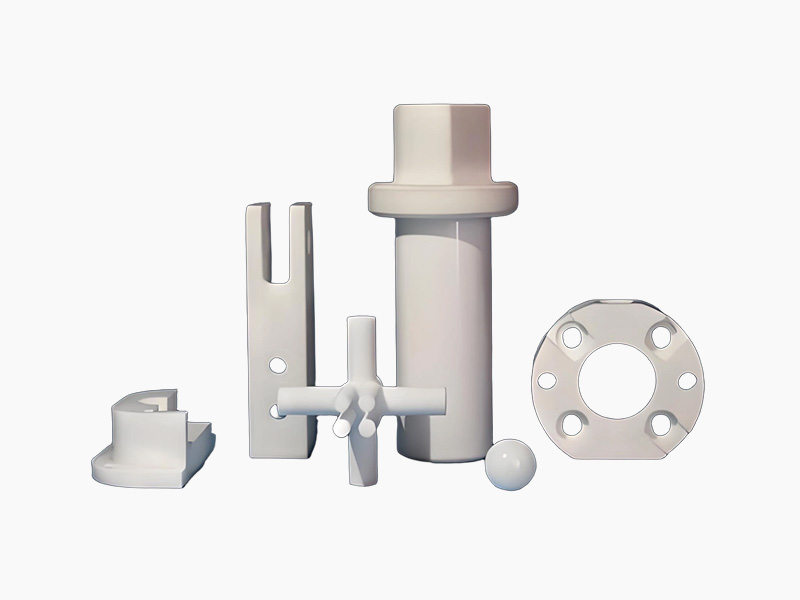
Si₃N₄ components used: Etch rings (focus rings), chamber liners, showerhead plates, gas distribution plates, upper/lower electrodes, and wafer clamping rings. These components must resist continuous bombardment by fluorine, chlorine, and bromine-based plasma species while maintaining dimensional stability and generating minimal particles. Si₃N₄ etch rings typically last 2-3× longer than quartz equivalents in standard CF₄/SF₆ etch processes.
② CVD / PVD Deposition Systems
Chemical vapor deposition (CVD) and physical vapor deposition (PVD) systems deposit thin films on wafers at elevated temperatures (300-1000°C) under vacuum or controlled gas atmospheres.
Si₃N₄ components used: Susceptor plates, heater covers, chamber shields, target shields, wafer lift pins, and insulating standoffs. In LPCVD processes where Si₃N₄ films are themselves deposited (using SiH₂Cl₂ + NH₃), the ceramic components must resist coating buildup and enable easy cleaning without degradation. Si₃N₄'s thermal stability and low outgassing make it ideal for these ultra-clean environments.
③ Lithography & Alignment Systems
Lithography is the most precision-critical step in semiconductor fabrication, requiring overlay accuracy of<1-2 nm for advanced nodes. Positioning mechanisms demand materials with exceptional dimensional stability.
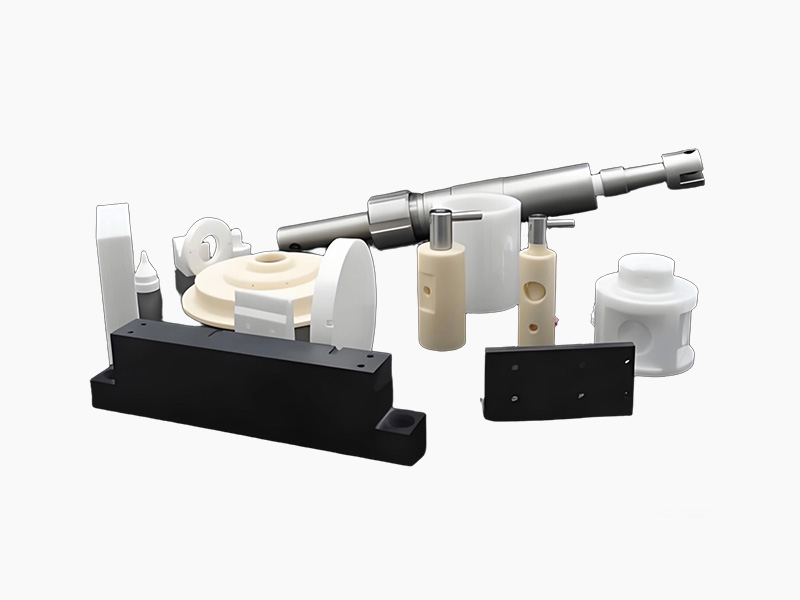
Si₃N₄ components used: Positioning/locating pins, alignment fixtures, wafer stage components, and precision guide elements. Si₃N₄'s combination of high stiffness (E ≈ 310 GPa), near-zero creep, and excellent wear resistance ensures that alignment accuracy is maintained over millions of positioning cycles. Its service life is 5× longer than zirconia locating pins and 40× longer than metal pins in precision positioning applications.
④ Chemical Mechanical Planarization (CMP)
CMP combines chemical etching and mechanical abrasion to achieve atomic-level planarity across the wafer surface - essential for multi-layer device architectures.
Si₃N₄ components used: Retaining rings, dresser boards, and conditioning disk substrates. The ceramic's exceptional hardness (HV 13-17 GPa) and wear resistance ensure consistent down-force distribution and slurry interaction over extended polishing cycles, directly contributing to within-wafer non-uniformity (WIWNU) targets of<1%.
⑤ Wafer Handling & Cleanroom Automation
Automated wafer handling robots transfer 300mm (and increasingly 450mm) wafers between process chambers at high speed, requiring end effectors that are lightweight, stiff, particle-free, and ESD-safe.
Si₃N₄ components used: Robot arm end effectors (blades/forks), wafer boat components, FOUP (Front Opening Unified Pod) parts, and EFEM (Equipment Front-End Module) structural elements. Si₃N₄'s 40% weight advantage over steel reduces robot inertia, enabling faster wafer transfer speeds while maintaining positioning accuracy.
⑥ Advanced Packaging & Testing
Advanced packaging technologies - including 2.5D/3D integration, TSV (Through-Silicon Via), fan-out wafer-level packaging (FOWLP), and chiplet architectures - demand new ceramic solutions.
Si₃N₄ components used: Bonding tool inserts, test socket components, die attach fixtures, and thermal management substrates. Si₃N₄ ceramic substrates are increasingly used for power module packaging in wide-bandgap (SiC/GaN) semiconductor devices, where the CTE match between Si₃N₄ and silicon chips (~3.2 vs 2.6 × 10⁻⁶/°C) reduces thermomechanical stress during power cycling.
Si₃N₄ Components in a Plasma Etch Chamber - Cross-Section Diagram
The following cross-sectional diagram illustrates the key positions where silicon nitride ceramic components are deployed within a typical inductively coupled plasma (ICP) etch chamber - one of the most critical pieces of equipment in semiconductor fabrication. Each labeled component represents a specific Si₃N₄ application point that leverages the material's plasma resistance, thermal stability, and dimensional precision.
Si₃N₄ Components in a Plasma Etch Chamber
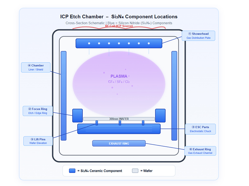
① Showerhead
Distributes process gases uniformly. Si₃N₄ resists plasma back-sputtering and maintains hole geometry.
② Focus Ring
Controls plasma sheath at wafer edge. Critical for etch uniformity. Highest erosion-rate component.
③ ESC Components
Electrostatic chuck insulating layers. Si₃N₄ provides dielectric isolation with thermal conductivity.
④ Chamber Liner
Protects chamber walls from plasma and deposition. Enables quick clean/replace maintenance cycles.
⑤ Lift Pins
Raise/lower wafers for robot transfer. Si₃N₄ provides wear resistance and zero metallic contamination.
⑥ Exhaust Ring
Gas exhaust flow control. Si₃N₄ resists corrosive byproduct gases and extends PM intervals.
Material Comparison: Si₃N₄ vs Other Semiconductor Ceramics
The following table compares silicon nitride with other commonly used ceramics in semiconductor equipment, helping engineers evaluate the optimal material for specific applications:
| Property | Si₃N₄ | Al₂O₃ | AlN | SiC | Quartz |
|---|---|---|---|---|---|
| Density (g/cm³) | 3.2-3.4 | 3.9 | 3.3 | 3.2 | 2.2 |
| Flexural Strength (MPa) | 700-1000 ★ | 300-630 | 300-500 | 400-600 | 50-70 |
| Fracture Toughness (MPa·m½) | 6-8 ★ | 3-5 | 2.5-3.5 | 3-5 | 0.7-1.0 |
| Thermal Conductivity (W/m·K) | 20-30 | 24-30 | 170-200 ★ | 120-270 | 1.4 |
| CTE (×10⁻⁶/°C) | 3.2 ★ | 8.1 | 4.5 | 4.0 | 0.55 |
| Plasma Erosion Resistance | Excellent ★ | Excellent | Good | Excellent | Poor |
| Thermal Shock Resistance | Excellent ★ | Moderate | Good | Good | Excellent |
| Relative Cost | High | Low ★ | Very High | High | Low |
| Best For | Toughness + thermal cycling + plasma | Insulation + cost-sensitive | Thermal management | Hardness + thermal conductivity | Transparency + low-cost |
★ = Best performance in this category among compared materials. Values are typical ranges for engineering-grade sintered ceramics.
Key Insight: Si₃N₄ occupies a unique position in semiconductor ceramics - it is the only material that simultaneously delivers the highest fracture toughness, excellent thermal shock resistance, and outstanding plasma erosion resistance. This combination makes it irreplaceable for components that experience both mechanical stress and plasma exposure, such as focus rings in high-power etch tools and wafer handling end effectors.
Manufacturing Process for Semiconductor-Grade Si₃N₄ Components
Producing semiconductor-grade Si₃N₄ components demands far more stringent quality control than standard industrial ceramics. The manufacturing process must ensure ultra-high purity, controlled microstructure, and sub-micrometer dimensional accuracy. Here is the typical production flow:
Powder Prep
High-purity Si₃N₄ powder (>99.9%) with Y₂O₃/Al₂O₃ sintering aids. Metallic impurities<1 ppm.
Forming (CIP)
Cold isostatic pressing at 200-300 MPa for uniform green body density and near-net shape.
GPS / HIP Sintering
Gas pressure sintering or HIP at 1750-1900°C. Achieves >99.5% theoretical density.
CNC Machining
Diamond grinding, lapping, polishing to ±1μm. Cleanroom-compatible surface finish (Ra<0.1μm).
QC & Packaging
100% inspection. Particle counting, ICP-MS purity analysis. Cleanroom vacuum packaging.
Extended Knowledge - Surface Finish for Semiconductor: Semiconductor-grade Si₃N₄ components typically require surface roughness (Ra) values of <0.2 μmto minimize particle trapping and enable effective wet cleaning. Some applications (e.g., ESC dielectric layers) demand Ra<0.05 μm. The final polishing step uses colloidal silica or diamond slurry in a cleanroom environment to prevent contamination.
Future Outlook: Si₃N₄ in Next-Generation Semiconductor Manufacturing
As the semiconductor industry advances toward sub-2nm nodes, 3D NAND with >300 layers, and heterogeneous integration architectures, the demands on equipment materials will only intensify. Silicon nitride ceramics are positioned at the center of several emerging technology trends:
EUV Lithography Era
EUV (13.5nm) lithography systems require ultra-pure, ultra-stable ceramic components for mask handling, wafer stages, and vacuum chamber internals. Si₃N₄'s low outgassing and dimensional stability make it a candidate for EUV-specific applications.
Si₃N₄ as a Thin-Film Material
Beyond structural components, Si₃N₄ is itself deposited as a thin film (via LPCVD/PECVD) on wafers as a gate dielectric, etch stop layer, passivation layer, and stress liner in strained-silicon technology.
Si₃N₄ Photonic Integrated Circuits
The Si₃N₄ photonic platform is emerging as a key technology for on-chip optical interconnects, quantum computing, LiDAR, and biosensing - leveraging the material's wide transparency window (visible to mid-IR) and CMOS compatibility.
Wide-Bandgap Power Electronics
Si₃N₄ ceramic substrates are critical for SiC and GaN power module packaging, where their CTE match, thermal cycling reliability, and high-temperature capability outperform traditional Al₂O₃ and AlN substrates in automotive and industrial power applications.
Conclusion
Silicon nitride ceramics have become an indispensable material in modern semiconductor manufacturing equipment. Their unique combination of plasma erosion resistance, ultra-low particle generation, thermal shock stability, mechanical toughness, and chemical inertness makes them the optimal choice for the most demanding process environments - from plasma etching and CVD/PVD deposition to lithography alignment and CMP processing.
As semiconductor technology advances toward smaller nodes, 3D architectures, and heterogeneous integration, the role of Si₃N₄ will only grow. Equipment OEMs and fab operators who invest in understanding and optimizing their use of Si₃N₄ ceramic components will gain significant advantages in yield, uptime, and total cost of ownership.
Xiamen HUACIJULI New Material Co., Ltd. stands ready as a trusted manufacturing partner, providing semiconductor-grade Si₃N₄ components engineered to meet the exacting specifications of the world's most advanced fabrication facilities. With decades of ceramic engineering expertise and comprehensive custom design capabilities, we deliver the precision, purity, and performance that the semiconductor industry demands.
Frequently Asked Questions (FAQ)
Q1: Why is silicon nitride used in semiconductor equipment?
Silicon nitride (Si₃N₄) is used because it offers exceptional plasma erosion resistance, high purity with minimal particle generation, excellent thermal stability up to 1400°C, superior fracture toughness (6-8 MPa·m½), and outstanding electrical insulation. These properties make it ideal for wafer processing chambers, etch rings, focus rings, showerhead plates, and precision positioning components.
Q2: What semiconductor equipment components are made from Si₃N₄?
Key components include etch rings/focus rings, showerhead plates, chamber liners, ESC parts, wafer lift pins, positioning/locating pins, CMP retaining rings, wafer handling end effectors, and CVD/PVD susceptor components. Si₃N₄ is also used as thin-film dielectric and etch stop layers deposited directly on wafers.
Q3: How does Si₃N₄ compare to other ceramics in semiconductor applications?
Si₃N₄ offers the highest fracture toughness (6-8 vs 3-5 MPa·m½ for Al₂O₃) and superior thermal shock resistance among semiconductor ceramics. It has lower thermal conductivity than AlN and SiC but compensates with better mechanical reliability. Its CTE (3.2 × 10⁻⁶/°C) closely matches silicon (2.6 × 10⁻⁶/°C), reducing thermomechanical stress.
Q4: What is the role of Si₃N₄ in wafer fabrication?
Si₃N₄ serves dual roles: as a structural material for equipment components (etch rings, chamber parts, positioning pins) that resist plasma and chemical attack, and as a thin-film material deposited on wafers via LPCVD/PECVD for use as gate dielectrics, etch stop layers, passivation, and stress liners in advanced CMOS processes.
Q5: How long do Si₃N₄ components last in semiconductor equipment?
Si₃N₄ components typically last 2-3× longer than quartz equivalents in plasma etch environments and 5× longer than zirconia positioning pins. In wafer handling applications, service life can exceed 40× that of metal components. The exact lifetime depends on process chemistry, plasma power, temperature, and duty cycle - but Si₃N₄ consistently ranks among the longest-lasting ceramic options.