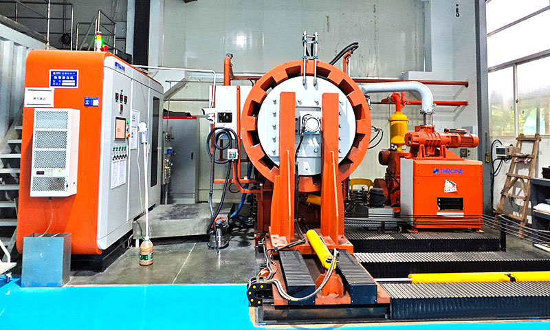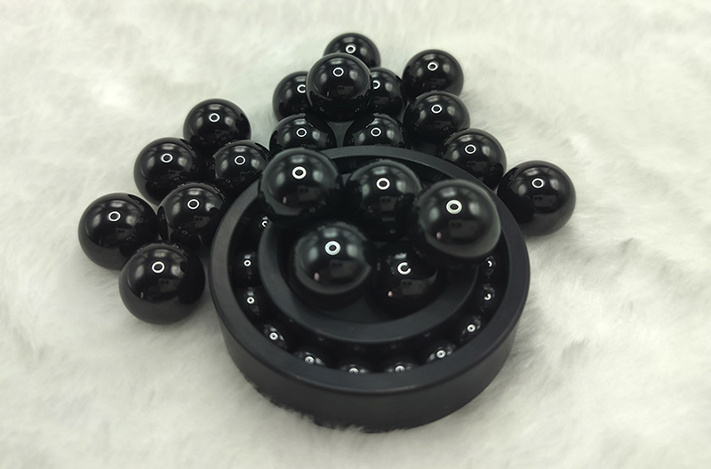

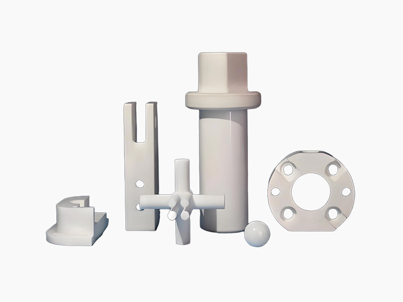
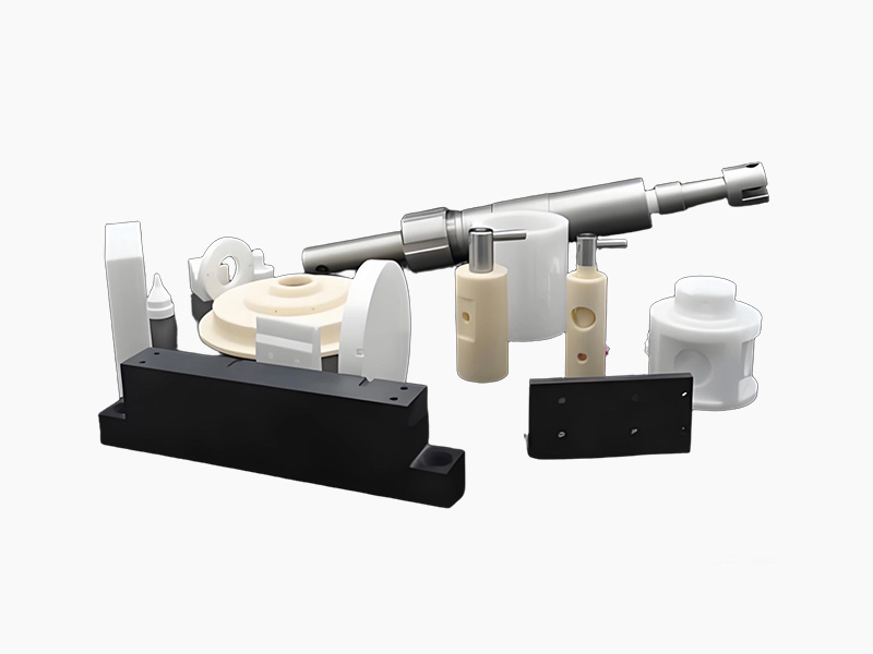
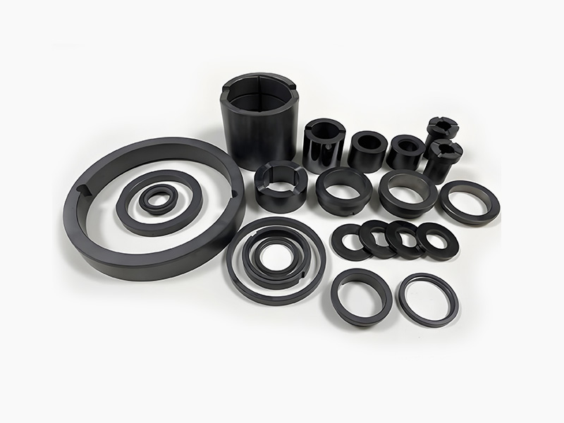


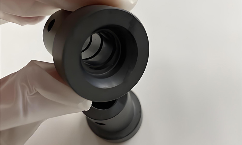
The semiconductor industry demands extreme precision, cleanliness, and reliability. Silicon nitride ceramic pins have become essential components in this field due to their unique material properties.
One of the primary uses of these pins is in wafer handling systems. During the manufacturing process, silicon wafers must be transported and positioned with micron-level accuracy. Silicon nitride ceramic pins provide the necessary precision while minimizing contamination risks, thanks to their non-reactive and non-metallic nature.
Another critical application is in vacuum environments. Semiconductor fabrication often takes place under vacuum conditions, where outgassing and material stability are major concerns. Silicon nitride exhibits low outgassing and maintains its structural integrity, making it ideal for such environments.
Thermal performance is also crucial in semiconductor processes, such as chemical vapor deposition (CVD) and plasma etching. Silicon nitride ceramic pins can withstand high temperatures without deformation, ensuring consistent positioning and alignment of components.
Furthermore, these pins contribute to equipment longevity. Their wear resistance reduces the frequency of maintenance and replacement, which is vital in semiconductor fabs where downtime can be extremely costly.
Electrostatic discharge (ESD) control is another area where silicon nitride ceramic pins offer advantages. While they are insulating, their controlled surface properties can be engineered to minimize static buildup, protecting sensitive electronic components.
The adoption of silicon nitride ceramic pins in semiconductor manufacturing reflects the industry’s need for materials that can meet increasingly stringent performance requirements. As technology continues to advance, their role is expected to expand further.